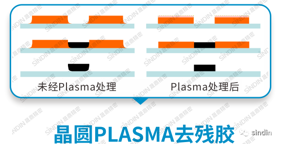
What is semiconductor wafer plasma debonding?

In semiconductor processing and other thin film processing processes, plasma removal of various photoresists is used to remove surface pollutants from materials and ensure their bonding ability with other materials.
What other applications do microwave plasma have besides glue?
FC packaging microwave plasma treatment
Before metal bonding
Wafer surface activation
SINDIN independently develops and controls core technologies
The first domestically independently developed microwave semiconductor debonding generator technology;
Magnetic fluid rotating frame ensures even processing effect;
Microwave non discharge electrode, efficient and uniform, ensuring etching rate;
Low temperature plasma to avoid thermal damage;
Low self bias requirement, compatible with microwave junction and magnetic circuit.


